Zero to Pcb: Overview
In this blog series I will cover the steps required to go from an idea to a pcb. Together we will build a simple LED badge which you can manufacture and wear.
Prerequisites
While not complete if you fall into one of these categories you should be able to get through the series without issue.
- you studied computer science
- you have built circuits on a breadboard or equivalent
- you have tinkered with dev boards (Arduino, Raspberry Pi)
- you remember your high school circuits class really well
Resources
- AllAboutCircuits.com has a wonderful textbook, it has just about everything you need to get started.
What this post covers
This blog post will cover the high level of what a pcb is and an overview of the steps needed to go from idea to production.
What is a printed circuit board (pcb)?
A pcb is a circuit made by stacking non conductive material and copper to create electrical connections. Pcb's provide a surface to mount components and be assembled into other things.
Below is a printed circuit board (teensy 4.0)
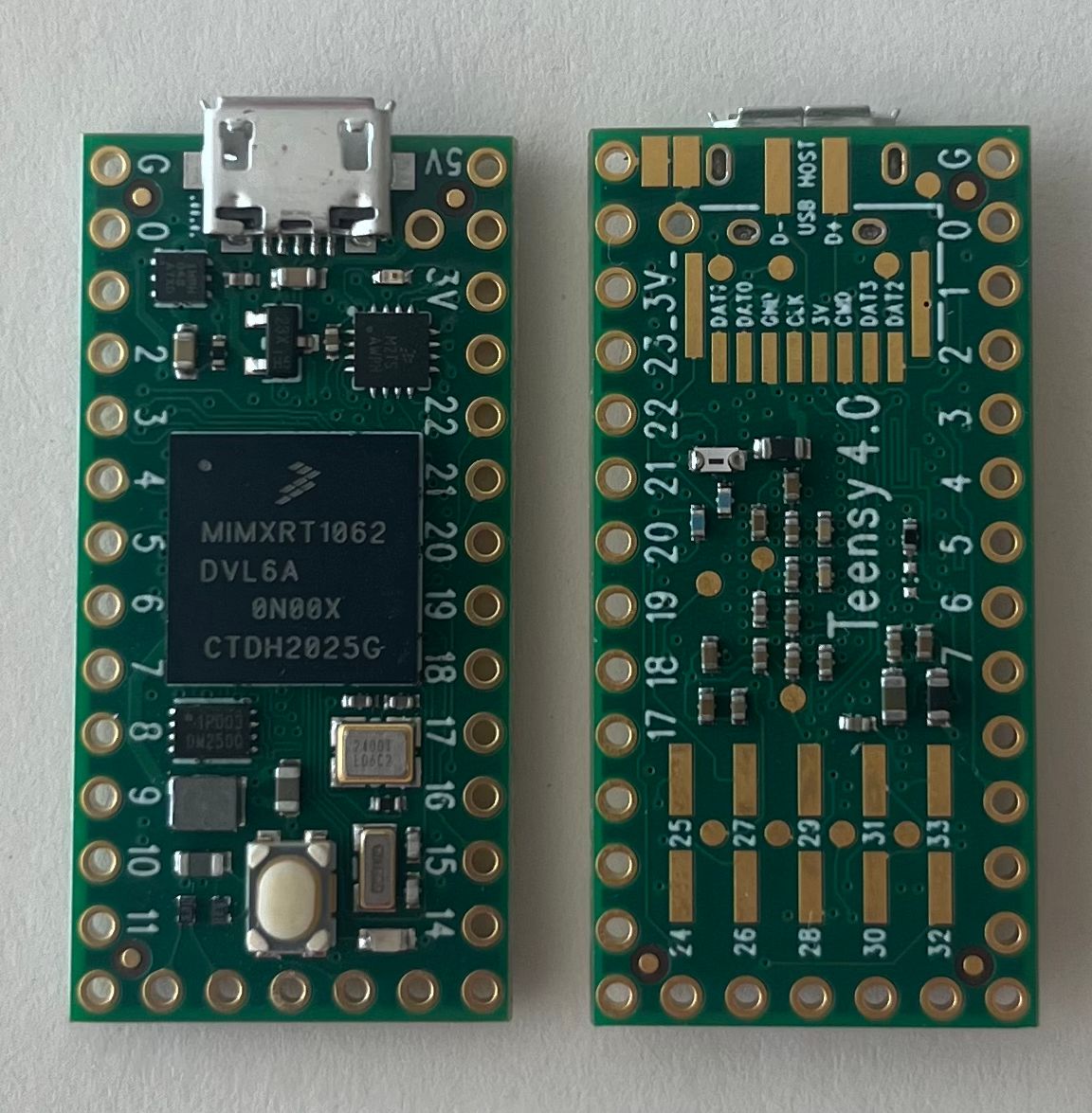
The non conductive material is the green and the copper is the exposed gold. If you look closely you will see some lines going all over the board, this is also copper but under some non conductive material called solder mask.
You will also see a bunch on things on top of the pcb like the usb connection (top left), a small button (bottom left), and a bunch of other rectangles on the board. These are known as components and are placed on the pcb after the layers of non conductive material and copper are squished together. They are typically soldered on and finish the pcb. More on the manufacturing process later.
Other examples of pcb's
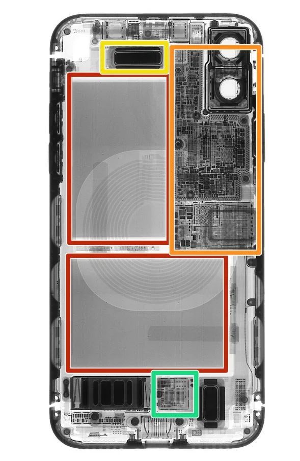
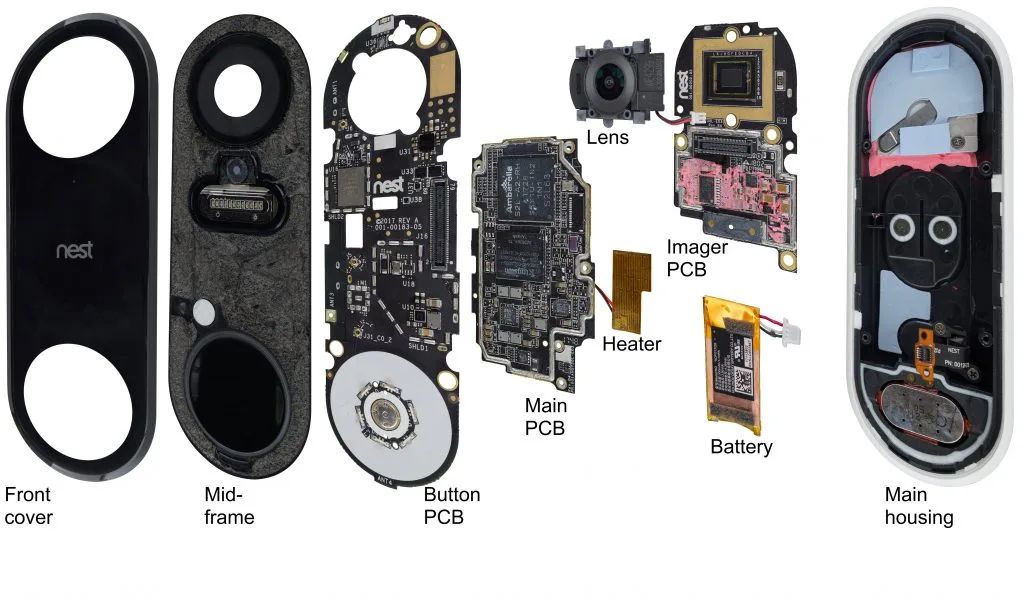
These days anything that is electronic likely has a pcb.
Your phone
Your laptop

Your doorbell toaster
Pcb alternatives
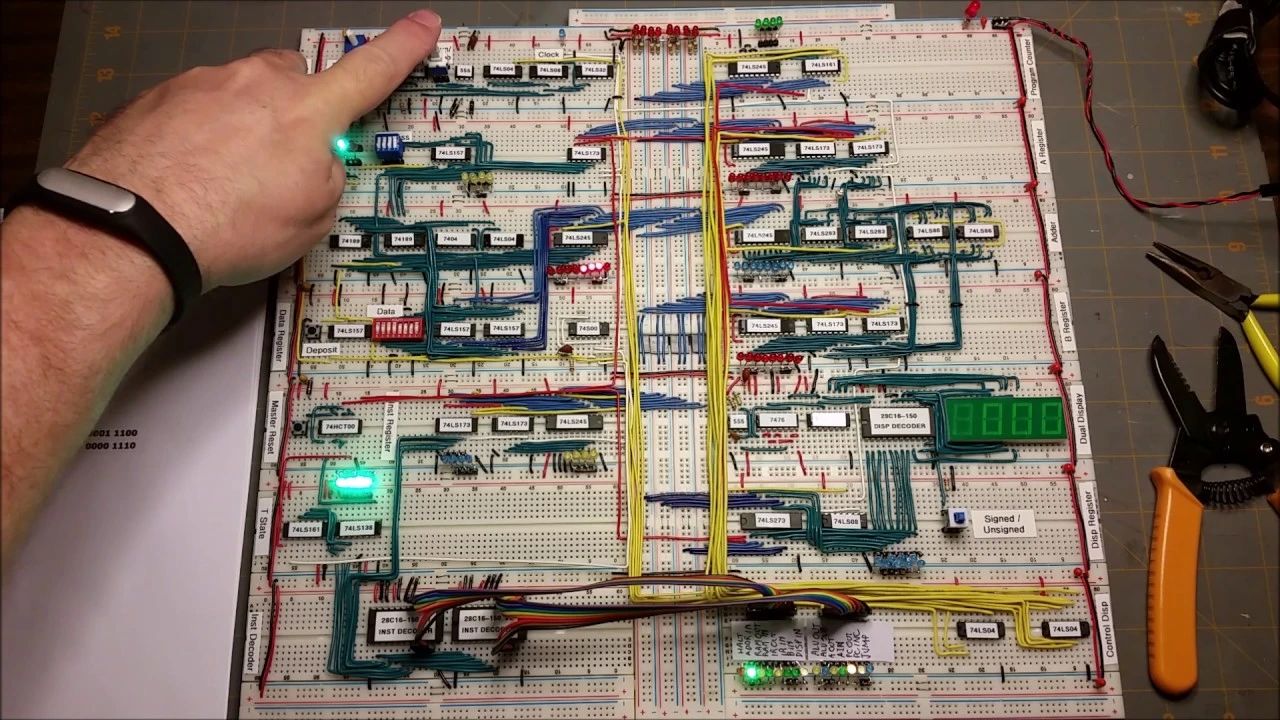
Before pcb's, circuits were made by point to point wiring. In point to point wiring you connect your components by soldering individual wires between them. This was often labor intensive and error prone. Furthermore, as the non conductive wrapping around the wire would age it would become brittle and break leading to exposed wire and short circuits.
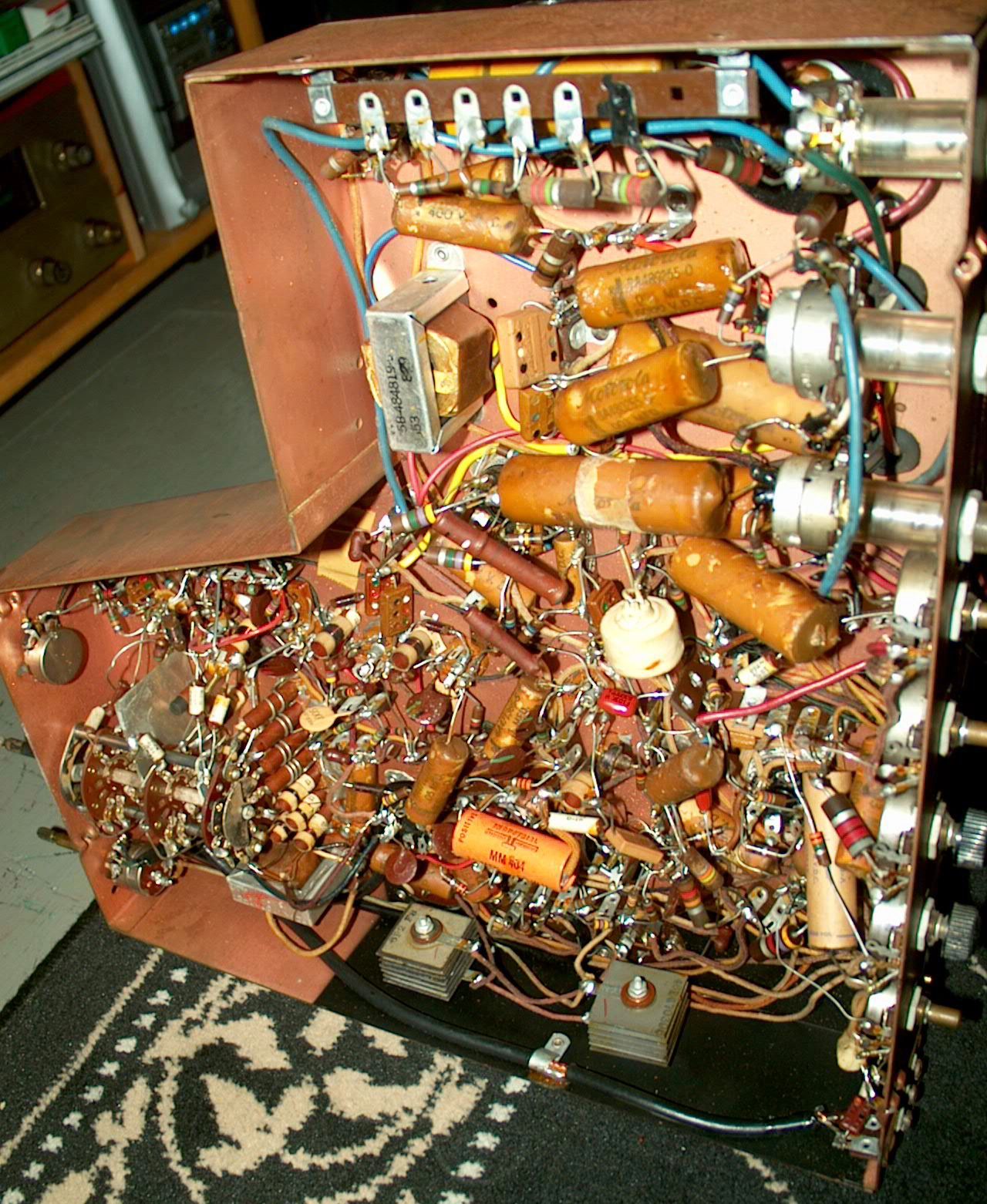
If you have ever worked on a breadboard you are essentially doing point to point wiring but without the soldering.
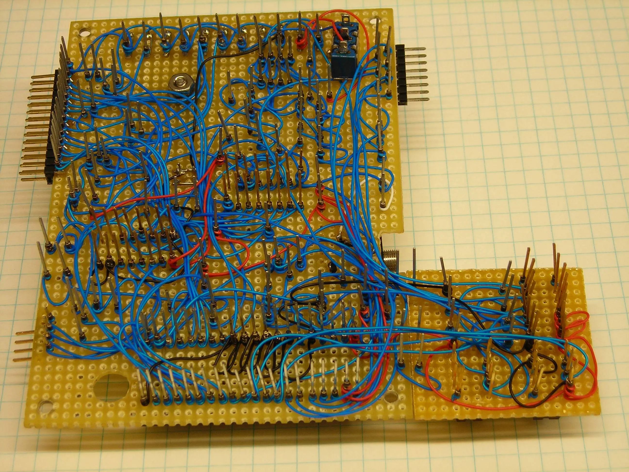
Another way of creating circuits was wire wrapping. In wire wrapping your components were mounted on a board with many small holes through it. Your component would have long conductive pins which would go through those holes. Connections between components were made by physically wrapping the exposed end of wire around the pins of the components.
Hackaday has a great deep dive on wire wrapping
Idea to Pcb: Overview
At a high level the process looks like this
graph LR
idea["Ideation"]
req["Requirements"]
block["Block Diagram"]
comp["Component Selection"]
sch["Schematic"]
pcb["Pcb Layout"]
manu["Manufacture"]

idea-->req-->block-->comp-->sch-->pcb-->manu
- Ideation & Requirements
- You have an idea for a circuit your would like to make
- Formalize a set of requirements for the circuit
- Block Diagram
- Break the circuit down into logical blocks
- Component Selection
- Choose a set of components which help realize that block diagram
- Schematic
- Wire the components together (adding more components are necessary) to realize the block diagram
- Layout
- Determine the size and shape of the board
- Figure out where the components are going to be placed on the board
- Route traces between the components to match the schematic
- Manufacture
- Choose a company to manufacture your board and send your CAD files to them
- Order components
- Solder your components onto your board
- Test and Debug
Example
Lets go through an example of the first couple of steps to get the idea. Lets propose I am a vampire, I am lazy and I don't like getting up during the day to close my blinds (so I don't burn). I can't keep them closed all the time because I like the moonlight at night. What if I could design a device which opens and closes the blinds depending on if the sun is up or not? (Ideation done)
The device would need to be able to:
- open and close my blinds
- detect if the sun is out or not
Looking around my lair I can refine my idea / requirements
- My blinds open and close by twisting a handle, a motor or servo should be able to handle that. This means I will need some circuit to control a servo and it will need electricity.
- All my windows have outlets next to them, I can power this device from the wall.
Lets draw the things that make up our design
graph LR
sun["Sun Detector"]
controller["Servo Controller"]
servo["Servo"]

sun<-->controller<-->servo
Pretty simple right?
Now we will look for some things to help us realize this.
For detecting if its day or night we can use a photoresistor. This is a small, cheap component which changes its resistance (ohms) depending on the amount of light reaching it surface. If there is a large amount of light it will have little resistance, if no light it will have a high resistance.
We need a way of converting that resistance into a yes / no, day / night. For this we will use a comparitor. If the voltage going through the photoresistor is less than the voltage going into the other input of the comparitor, the comparitor will output high. This high signal will indicate that its daytime.
Given this day / night signal we can put the servo in two positions. Servos use voltage to determine their position so a simple switch should allow us to use the day / night signal to change between two voltages.
We now have a list of components which we can wire up together in real life or in a schematic.
We can then take that schematic and lay it out on a pcb.
Reality
In reality the circuit is unlikely to be perfect right away and the high level process diagram isn't a straight line. You will often have to revise an earlier step in the process as things come up.
For example, we built our board and set up our blinds to use it and found that "Oh no! The moon is too bright at night and keeps the blinds closed". We need a way to adjust the comparitor. We will have to look at our circuit and determine a way to do that, then pick parts for it, then adjust the schematic and pcb. In the example above we can adjust the other input to the comparitor by using a poeteniometer, a device with variable resistance, this will allow us to modify how sensitive the circuit is to daylight before it outputs high.